Sunday 3 July 2016

Test Bench


whenever you need to store value you use reg
and whenever you have to just keep value you use wire

from test bench when you provide inputs then you can say that you have provided stimulas

If you see the above diagram you can see that you have to provide your stored value as input in your design module so you are bouded to use reg

whereas for analyzing the output you have to use wire

You should know that tool is use tool is use to see the simulation


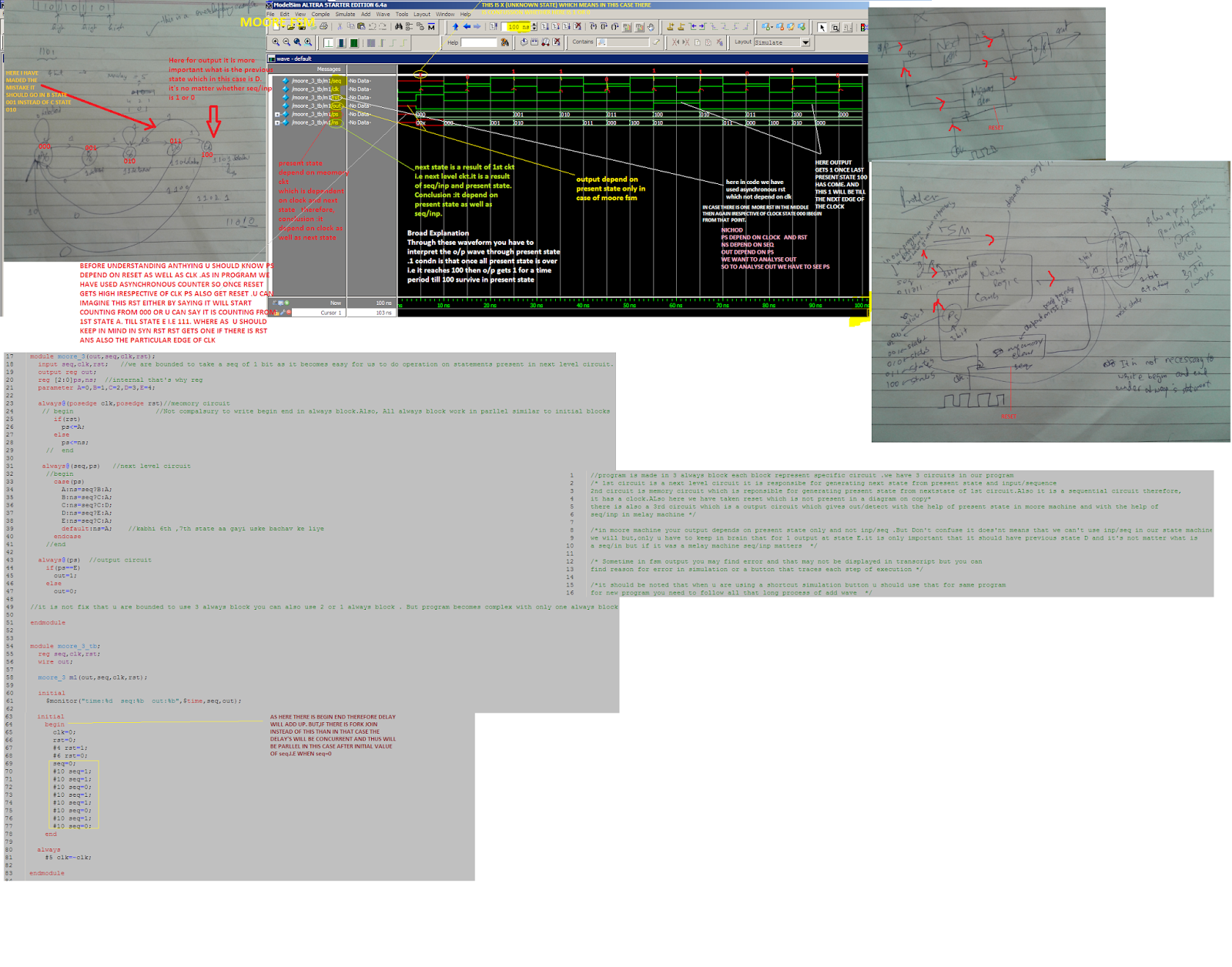
`include "and2.v"              //we extenstion is must  .v symbol

`timescale 1ns/100ps

this means it will consider #10 as 10 ns

`define clockperiodby2 10 //10ns half period is 50MHz
in above define commad you can use any name

the define command is use to assign this delay anywhere you like.For eg

clockperiodby2 clk=!clk;


when you sythesis your code in fpga you just burn design and thus there is no meaning of hash delay's .obivously as test benches are just an another way to test ur design through simulation other than FPGA. Anyway i also admity FPGA is more fun full way of testing your circuit.


It is safe to send data before posedge if you have it in your sensitiity list .Sending data after posedge makes no use


In always block you must use blocking assignment i.e <= and not "=" .However you can use any in intial block


Common Mistakes while writting test bench

Spelling of Initial

Ignoring Begin end


Anyway there are many beautiful way's of checking simulation

Using System Verilog {costilier way}--tools are crossing 1 lakh rupee

System C [Inspire from Circuit Sutra]---Basically company works on finding Verification Methodoly for Hardware design

Python scripts  [Inspire from Here]

Tuesday 21 June 2016

Inside CPU


Free Electricity at home

Telecome Industry Never tell you about the free electricity that they provide in your telephone lines


Wednesday 8 June 2016

COUNTERS

WHY COUNTERS ?

Ans. As clock just generate a pulse similarly counter generates a counting with the help of this pulse.

Note: In counter's we go from LSB to MSB  Q0--Q3
and while writing a sequence from waveform write carefully from MSB --LSB Q3--Q0
ASYNCHRONOUS COUNTER
--These are also Known as Ripple Counter
--As there is a more delay compared to synchronous there fore there comes a gliches in its waveforms
--Moreover in Asynchronous counter there is no combinational circuit in input so here
Tclk>=Tc-->q

Unlike synchronous counter having Tclk>=Tc-->q + Tpd(propogation delay of combination logic)

--In Asynchronous while making waveforms we have to just see the +ve edge of clock
   whereas
  In Synchronous you also have to see waveform of input of flipflop combinational logic apart from +ve edge of clock.


SYNCHRONOUS COUNTERS

These counters saves us from glitch waveforms all outputs in these are having same delay 
--FSM
--MOD COUNTER
--EVEN COUNTER
--ODD COUNTER


3-BIT SYNCHRONOUS COUNTER


4-bit Synchronous Counter


Difficult Synchronous Counter


Tuesday 31 May 2016

TPU

TPU (Tensor Processing Unit)


-->Google has said that this device is far away better than CPU,GPU,FPGA's.
-->This is far better from above devices as it uses less transistor per unit watt
-->But contrary some blogs says at same time it occupies more power
-->This is use to develop custom hardware
-->This will be attached to the Hardisk's at Google data centre
-->One can develop custom Hardware's Using these TPU access through cloud i guess.
-->Google street view and its deep mind technology Alpha Go (Chinese Game that represent human brain) works on this TPU.
--> It is 7 generation higher than More's Law
-->It is develop with an requirnment that great softwares needs beautiful hardware
-->It is discussed in I/O conference Google by CEO sundar pichai


Reference :-Google Blog

Watch Last few minutes of speech by CEO Sundar Pichai in below video


Sunday 22 May 2016

Interfaces (I2C ,SPI, RS232)

Interfaces are the protocols that are required by the devices to interact. Some of the common Interfaces are I2C,SPI,RS232 Interface.
Among three interface SPC is fastest after that comes I2C and finally RS232 which not has any clock. Watch below video to gain practical Knowledge too about above mentioned interfaces.Arduino has inbuilt SPC,I2C interface. and  Raspberrypi has inbuilt all interfaces. 

In below Video Ben Heck
Used SPC--to interface distance sensor with arduino
Used I2C--to interface temperature sensor with arduino
Used RS232--to interface Speaker using chip which too interfaced with the chip of RS232 which finally connected to computer where command were desired words were written to hear one by user.

Watch Below Video for better Understanding.


UART

Adding UART(Universal Asynchronous Receiver Transceiver


For More Information [Click Here]

UART
--UART is the universal Asynchronous Receiver Transiver
--It is the protocol is a self-syncronizer that is without synchronous clock with host (transceiver) the data automatically sends to the receiver.

To Understand the protocol of UART you should understand following terms

SPI Interface (Serial Peripheral Interface)--It is the protocol made by motorolla .this is a 4 wire serial communication .use to transfer data from peripheral to microcontroller/microprocessor or b/w microprocessor to microprocessor

 For More Info [Click Here]

FIFO MODE(First in First Out Mode)--It is the mode that is use in

For More Info [Click Here]

For More Knowledge from eye of chip designer Visit [Click Here] (Given Text in very interesting way)

Clock

Clock is the heart of any electronics hardware device that calculates,provides delay etc.Clock is essential in every hardware that needs a repetion like generating a ramp wave in multimeter, increasing or decressing a speed of processor, It is use almost in every device.

Clock is given using crystal oscillator, cmos ic etc.

Clock can be understanded better by student and bell example in schools

In Processor Clock impacts speed in following ways

---Raising a clock

---Dividing a clock by some factor (>1 i guess) i guess---gives more no. of cycles(Combination of each tick(1) tack(0) is known as cycle)-->fasten the speed

---Multiplying a clock by some factor (>1 i guess)---gives less no. of clock cycles (I guess if multiplication factor is greater than 1.obviously ! if it is less than 1 then it would indirectly be a division ...decimal removed ..no go down ...lab ! lab!. --> ultimately in these as time period increases therefore,no of clocks come after huge huge interval -->and thus speed reduces.

there are also many other factors to increase speed of processor beside clock like

--Pipelining
--Parllelism
--Increasing Cores of CPU
--Increasing No.  of bits like make a 64 bit ......the advantage of this reflects in high end graphics games....and not much in small programs....that is by increasing number of bits you mean to increase the data rate at a fix interval of time

For Detailed Knowledge [Click Here]

Thursday 19 May 2016

FSM


In above code you have maded two always{procedural} blocks because your “y” {past state} is a level sensitive in first always block and negedge clk is the edge triggered in your second always procedural block therefore,it is a rule you can’t write both edge triggered as well as level triggered in same sensitivity list.


Sunday 15 May 2016

Analysis of Timing Diagram in LCD Driver

Watch from 5:37


Kinds of Signal While Analyzing a Waveforms

Differntial Pair Signalling


you can see here we mix two different kinds of waves in it .

Why we use these kinds of signal?

Ans. Because you get much higher speed with these signals


Top Channels for Electronics Engineer


1.For Techical Seminars
CCCen
2.For Projects
Ben Heck Show


PSHDL

You can do PSHDL coding in cloud itself

In PSHDL if you just write


  1. module MyFirstModule{
  2. register uint<17> counter=counter+1;
  3. }


it means the system will count at rising edge of every count

But in case you want a register to count at falling edge then in that case you have to write code as follow:-


1) Adding a Two Number using PSHDL


Do you Know How Actually Simulation is coming out on Browser? The answer to this is you have converted your code into javascript.

2) Making a Counter Using PSHDL

  1. module MyFirstModule{
  2. register uint<17> counter=counter+1;
  3. out bit led=counter(13);
  4. }
And your output will be blinking led as shown on that screen


Now you can yourself see How simple is this PSHDL


Sunday 24 April 2016

Hexadecimal operations


Bit rate Vs Baud Rate

In digital Communication our Intention is to transfer Digital Data which is obviously seen in bit and therefore for that we use the term bit rate.

But As we can't send this digital data directly so for that we have to convert this digital data into some sought of signal and that is achieved by line coding techniques like NRZ, Manchester coding ....etc etc.
Now when we talk about speed here in sense of this signal then we talk about baud rate which is also known as pulse rate/ modulation rate/ baud rate or simply baud. 

You can also make a analogy of above concept as by a example of train where each carrier of a train is the signal element (baud) and passenger sitting inside that carrier is a data element (bit).
similarly signal rate (baud rate) and data rate(bit rate)

For Higher efficieny bit rate > baud rate
and To increase this efficiency only we have many line coding techniques

Formula for Baud rate is

Baud Rate = Bit rate
                     ------------
                     No. of data element carried by each signal element


There is some examples also for detail Understanding
For that [Click Here]

Saturday 23 April 2016

CPU VS FPGA VS ASIC

CPU---SOFTWARE--LIST OF INSTRUCTIONS
FPGA--FIRMWARE--GATES---PROGRAMED WITH THE HELP OF VERILOG,VHDL
ASIC--IT CAN BE USED AS FPGA BUT NOT REPROGRAMMED

it means you will test your design on fpga practically verify it and then give chip manufacturing industry to manufacture a chip.


Friday 22 April 2016

Microprocessor 8085 Verilog


  1. /*module processor(a,b, );
  2.   input [2:0]opcode;
  3.   input a,b;
  4.   output o;

  5. case(opcode)
  6.   begin
  7.   000: assign o<=a+b;
  8.   001: assign o<a-b;
  9.   010: assign 
  10.   */
  11.   
  12. module meomory(addr,,enable,out);
  13. input [2:0]addr;    //pc
  14. output reg [10:0] out;
  15. reg [10:0]mem[7:0];
  16. input enable;      //read
  17. initial
  18. $readmemb("input.txt",mem);
  19.   always @(*)
  20.   if(enable)
  21.  out=mem[addr];
  22.  else
  23.    out=out;
  24.    
  25. endmodule


  26. module ir(a,en,out);
  27.   input [10:0]a;
  28.   input en;
  29.   output reg [10:0]out;
  30.   always @(*)
  31.   begin
  32.     if(en==1)
  33.   out=a;
  34. end
  35. endmodule

  36. module decoder(in,en,opcode,data);
  37. input [10:0]in;
  38. input en;
  39. output reg [2:0]opcode; 
  40. output reg[7:0]data;
  41.   always @(*)
  42.   begin
  43.     if(en==1)
  44.       begin
  45.   opcode=in[10:8];
  46.   data=in[7:0];
  47.    end
  48.    /*else
  49.      begin
  50.      opcode=0;
  51.      data=0;
  52.     end*/
  53. end
  54. endmodule

  55. //module meomory_tb;
  56. //  reg [3:0]addr;
  57. //  reg enable;
  58.   
  59. module ir_tb;
  60.   reg [10:0]a;
  61.   reg en;
  62.   wire [10:0]out;
  63.   ir v1(a,en,out);
  64.   
  65.   initial
  66.     begin 
  67.       #1 en=1;
  68.       #5 a=11'b10001100110;
  69.       #10 en=0;
  70.       #11 a=11'b01011001101;
  71.   end
  72. endmodule

  73. module decoder_tb;
  74.   reg [10:0]in;
  75. reg en;
  76. wire [2:0]opcode; 
  77. wire [7:0]data;
  78. decoder v2(in,en,opcode,data);
  79.    initial
  80.      begin
  81.        #1 en=1;
  82.       #5 in=11'b10001100110;
  83.       #10 en=0;
  84.       #11 in=11'b01011001101;
  85.   end
  86. endmodule

  87. module alu4pro(opcode,vala,valb,aluout);
  88.   input [2:0]opcode;
  89.   input [7:0]vala;
  90.   input [7:0]valb;
  91.   output reg [10:0]aluout;
  92.   parameter add_op=3'b000,sub_op=3'b001,nand_op=3'b010,nor_op=3'b011,xor_op=3'b100,and_op=3'b101,or_op=3'b110,xnor_op=3'b111;

  93.   always @(*)
  94.   
  95.   case(opcode)
  96.   
  97.       
  98.     add_op: begin
  99.       aluout=vala+valb;
  100.     end
  101.     
  102.     sub_op:begin
  103.       aluout=vala-valb;
  104.     end
  105.     
  106.     nand_op:begin
  107.       aluout=~(vala&valb);
  108.     end
  109.     
  110.     nor_op:begin
  111.       aluout=~(vala|valb);
  112.     end
  113.     
  114.     xor_op:begin
  115.       aluout=vala^valb;
  116.     end
  117.     
  118.     and_op:begin
  119.       aluout=vala&valb;
  120.     end
  121.     
  122.     or_op:begin
  123.       aluout=vala|valb;
  124.     end
  125.     
  126.     xnor_op:begin
  127.       aluout=~(vala^valb);
  128.     end
  129.   
  130.   endcase
  131.     
  132. endmodule

  133. module alu4pro_tb;
  134.   reg [2:0]opcode;
  135.   reg [7:0]vala;
  136.   reg [7:0]valb;
  137.   wire [10:0]aluout;
  138.   alu4pro b2(opcode,vala,valb,aluout);
  139.   initial
  140.   begin
  141.     opcode=3'b000;
  142.     vala=3'b10;
  143.     valb=3'b11;
  144. #20opcode=3'b110;
  145. vala=3'b111;
  146. valb=3'b101;
  147. end
  148. //$monitor("time=%d,opcode=%b,vala=%b,valb=%b,aluout=%b",$time,opcode,vala,valb,aluout);
  149. endmodule

  150. module accumulator(aluout,clk,rst,accout);
  151.   input [7:0]aluout;
  152.   input clk;
  153.   input rst;
  154.   output reg [7:0]accout;
  155.   always@(clk)
  156.   if(rst)
  157.     begin
  158.      accout=aluout;
  159.   end
  160. else
  161.   accout=0;
  162. endmodule

  163. module accumulator_tb;
  164.   reg [7:0]aluout;
  165.   reg clk;
  166.   reg rst;
  167.   wire [7:0]accout;
  168.   accumulator b3(aluout,clk,rst,accout);
  169.   initial
  170.     begin
  171.       clk=0;
  172.       rst=1;
  173.       aluout=6'b101011;
  174.       #10 rst=0;
  175.       #15 rst=1;
  176.       
  177.     end
  178.       always #5 clk=~clk;
  179. endmodule
  180.  
  181. /*module controller();
  182.   output reg rd,rw,de,en;
  183.   reg ps,ns;
  184.  input clk,rst;
  185.   always @(clk)
  186. */
  187. module controller(rst,clk,read,addr,fe,de,ex);
  188.   input rst,clk;
  189.   reg [2:0]ps;
  190.   reg [2:0]ns;
  191.   output reg read,fe,de,ex;
  192.   parameter fetch=3'b000,decode=3'b001,execute=3'b010;
  193.   output reg [3:0]addr=4'b0000;
  194.   always @(posedge clk ,posedge rst)
  195.     if (rst)
  196.       ps<=fetch;
  197.     else
  198.       ps<=ns;
  199.     
  200. always @(clk)
  201.    case(ps)
  202.      fetch: begin
  203.        read=1;
  204.        fe=0;
  205.        de=0;
  206.        ex=0;
  207.     end
  208.     decode:begin
  209.       read=0;
  210.        fe=0;
  211.        de=1;
  212.        ex=0;
  213.      end
  214.      execute:begin
  215.       read=0;
  216.        addr=addr+1;
  217.        fe=0;
  218.        de=0;
  219.        ex=1;
  220.      end
  221. endcase
  222. endmodule


  223. module controller_tb;
  224.   reg rst,clk;
  225.   //reg[2:0]ns;
  226.   wire read;
  227.   wire fe,de,ex;
  228.   controller b1(rst,clk,read,fe,de,ex);
  229.   initial
  230.    begin
  231.      clk=0;
  232.      rst=0;
  233.      #10 rst=1;
  234.      #12 rst=0;
  235.     // #2 ns=3'b001;
  236.   end
  237.      always #5 clk=~clk;
  238. endmodule


  239. module processor(rst,clk,inp,outp);
  240.   input rst;
  241.   input clk;
  242.   input [10:0]inp;
  243.   output [10:0]outp;
  244.   wire accout;
  245.   wire rd;
  246.   wire ex;
  247.   wire de;
  248.   wire read;
  249.   wire addr;  //pc
  250.   wire mout; //meomory output
  251.   wire opcode;
  252.   meomory hk1(addr,read,mout); //read=enable
  253.   ir hk2(mout,rd,out);  //rd-enable  mout-a
  254.   decoder hk3(out,de,opcode,data); //de-enable
  255.   alu4pro hk4(opcode,inp,accout,aluout);    //decoder ka de 8bit data kaise use karon !!!! pehle hi ek acc se i/p ek main i/p donga is module se dusra i/p decoder wale ka kya karonga ...refer to diagram 
  256.   accumulator hk5(outp,clk,ex,accout);  //ex-rst
  257.   controller hk6(rst,clk,read,addr,fe,de,ex);
  258.   
  259. endmodule

  260. module processor_tb;
  261.   reg rst,clk;
  262.   reg[7:0]inp;
  263.   wire [7:0]outp;
  264.   processor hk10(rst,clk,inp,outp);
  265.   initial
  266.     begin
  267.       rst=0;
  268.       clk=0;
  269.       #2 inp=8'b01110101;
  270.       #5 rst=1;
  271.       #7 rst=0;
  272.     end
  273.     
  274.   always #10 clk=~clk;
  275. endmodule
simulation of proccessor_tb

Simulation of ir_tb


Simulation of decoder_tb


simulation of alu4pro_tb


simulation of controller_tb


simulation of accumulator_tb